64x32 SRAM Memory Chip

INTRODUCTION:
One of the primary memories used in today’s computers and smart devices is SRAM, which stands for Static Random Access Memory. This type of memory is very fast and can retain data bits as long as power is being supplied. In our course, we will be given the opportunity to design our own SRAM chip using EDA tools such as Synopsys Custom Compiler. The memory consists of various sub-blocks and interconnects that play specific roles in order for the SRAM to work as desired. These sub-blocks include: SRAM cell, SRAM array, pre-charge circuit, sense amplifier, write driver, row decoder, and controller (Figure 1). Each of these components are explained in more detail in the following sections. We will also be discussing the process of how we integrated the blocks and the results that we accomplished. The goal of this project is to achieve minimal: layout area, access time, and/or active power consumption.
.png)
Figure 1: Design Architecture of SRAM Chip.
CELL:
The 6-T SRAM cell can be considered to be the heart of the SRAM memory chip. It consists of six transistors: two access transistors, two pull-up transistors, and two pull-down transistors (Figure 2). The pull-up and pull-down transistors create two feedback inverters opposite from each other which allow the cell to store one bit of memory, either a 1 or a 0. The access transistors can be seen as the doors of the cell. When turned on, they allow current to flow either in or out of the cell depending on whether it’s a read or write operation.

Figure 2: SRAM Cell Schematic.
It may sound simple, however it gets complicated fairly quickly as there is more to just creating a schematic. Each transistor needs to be sized to a certain width in order for the cell to operate as desired. You begin by setting the pull-up transistors to a minimum size (0.24 um) and tuning the pull-down transistor until you measure an SNM (Sound Noise Margin) of 100 mV on the WaveView (Figure 3). The access transistors can also be tuned to help attain the anticipated SNM. We sized our pull-down transistors to 0.405 um and access transistors to 0.335 um.
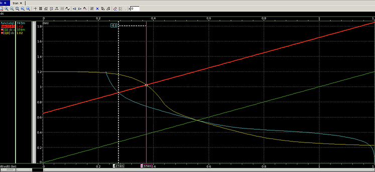
Figure 3: Static Noise Margin measurement.
Now that the SRAM cell transistor sizes are determined, we now need to measure the bitline delay by creating a testbench (Figure 4) and performing transient analysis. The bitline delay is the delay from the time the word-line rises to the time bitline drops by 100 mV. In our case, we obtained a bitline delay of 27.7 ps (Figure 5).
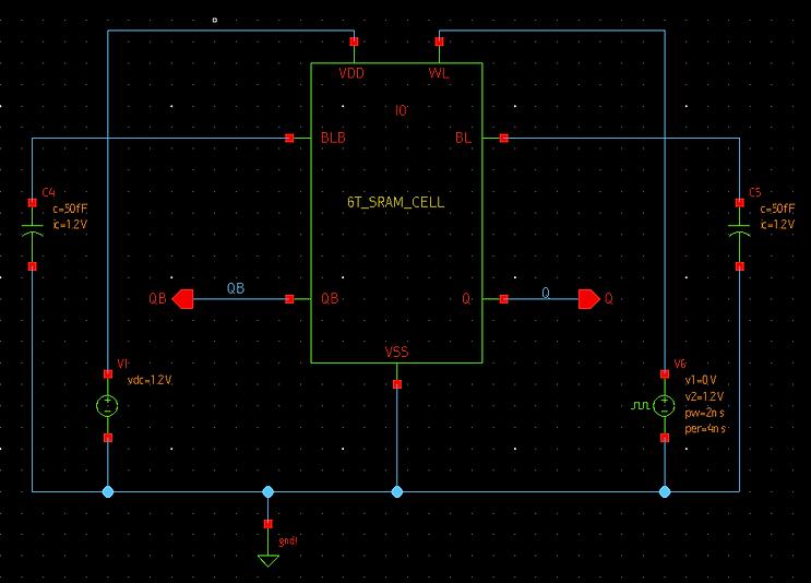
Figure 4: Testbench used to measure bitline delay.

Figure 5: Bitline delay measurement.
Now that the SRAM cell transistor sizes are declared, tested, and satisfied, you can now proceed onto the layout design. It is important to note that you do not want to begin layout until you have set transistor sizes because if you change the sizes in the schematic you will also need to change them in the layout which can take a long time to fix and optimize. The layout step is a chance for you to get creative and show off your design skills. You may design it however you’d like as long as it passes the Design Rules Check (DRC) and Layout Vs Schematic (LVS) tests. Although you are given this freedom, you still want to create a design that is as compact as possible in order to achieve a small area and that will fit to other components of the SRAM. In our case, we obtained an SRAM cell layout area of 3.36 um2 (Figure 6). We referring heavily to the Design Rules Document which states all the minimum distances between layout layers.

Figure 6: SRAM Cell layout.
SRAM ARRAY:
The SRAM array is made out of 64 rows and 32 columns of SRAM cells. Therefore, in order to create the array you first need to complete the individual cell. In the array schematic, you need to connect the cell bitlines in each column together and the cell word lines together in each row. You also need to connect all the VDD ports together and VSS ports together for each cell (Figure 7). Although it doesn't make a difference in the schematic I connected the SRAM cells just like I connected them in the layout so that it is easier to understand (Figure 8).
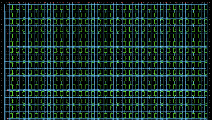
Figure 7: SRAM Array schematic (far view).

Figure 8: SRAM Array schematic (close view).
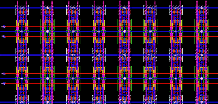
The layout procedure is similar as the SRAM cell layout where you just need to make sure that you pass the DRC and LVS. In order to reduce area, we used the overlap method as shown in Figure 8 where we connect the VSS nodes of two cell rows together and the VDD nodes together with the following row. In other words, every pair of cell rows are sharing a VDD and a VSS node. You can get a closer look at the method in Figure 9. Figure 10 shows a zoomed out view of the array layout.
Figure 9: SRAM Array layout connections (overlap method).

Figure 10: SRAM Array layout (far view).
PRE-CHARGE CIRCUIT:
When we want to perform the read operation, certain actions occur in order for us to read the values that are stored in the specified address. One of those actions involve the pre-charge circuit. The purpose of the pre-charge circuit is to charge the bitlines of each column to VDD (1.2 V) before the word line is turned on by the row decoder. Once the bitlines are charged and the access transistors are turned on (word line goes high), either BL (BitLine) or BLB (BitLine Bar) will experience a voltage difference. This difference will be picked up by the sense amplifier that is located at the bottom of the array and will output the values stored in each cell.
The pre-charge circuit consists of three PMOS transistor: two bitline transistors and one equalizer transistor. The bitline transistors are connected directly on the bitlines where the equalizer transistor is connected between them, almost as creating a bridge (Figure 11). The purpose of the equalizer transistor is so that both bitlines, BL and BLB, obtain equal potential when being charged to 1.2 V. The gates of all three transistors are connected together so that they turn on simultaneously when called by the controller.

Figure 11: Pre-charge circuit schematic.

Again we need to tune the sizes of each transistor so that the pre-charge circuit can operate as expected. In this case, we want the pre-charge circuit to charge the bitlines to VDD as fast as possible (small pre-charge delay). To determine these sizes, we created a testbench that connects a single pre-charge circuit to ‘dummy’ access transistors as if it were connected to actual SRAM cells (Figure 12). We also multiplied those those transistors by 64 so that the load on the bitlines can be similar for when it is actually connected to the array.
Figure 12: Testbench used to measure bitline delay.
In the testbench, the pre-charge enable (“PRECHARGE”) and the access transistors’ gates are connected to the same pulse generator. When the signal is low, the access transistors are off, the pre-charge is enabled, and the bitlines are charged to VDD. When the signal goes high, the pre-charge circuit is turned off and the access transistors are turned on causing the bitlines to be drained to 0. The signal then goes high and the cycle is repeated again. The delay from the time the pre-charge is enabled to the time the bitlines charge up to 1.2 V is called the pre-charge delay. We sized our bitline transistors to be 1.0 um and our equalizer transistor to be 0.24 um. These sized allowed us to achieve a pre-charge delay of 333 ps, which can be seen in Figure 13, and proceed to the layout task (Figure 14).

Figure 13: Pre-charge delay measurement.

Figure 14: Pre-charge layout.
Once the pre-charge circuit is set, we now need to create a 32 column pre-charge circuit chain to connect on top of the SRAM array. Each bitline will connect to its designated bitline in the array so that the circuit can charge them when enabled. Figures 15 and 16 are far and close views of the schematic and Figure 17 is its layout form.

Figure 15: 32 column pre-charge circuit (far view).

Figure 16: 32 column pre-charge circuit (close view).

Figure 17: Pre-charge circuit column layout.
SENSE AMPLIFIER:
Our main goal is to design a sense amplifier that is small in area but fast enough for the overall function of the SRAM. Each column of the SRAM array consists of one sense amplifier that is located at the very bottom. It’s similar to the pre-charge circuit that is located at the top of the array but instead is at the bottom of the array. The type of sense amplifier we are using is called Current Controlled Latch Sense Amplifier and consists of four PMOS transistors and five NMOS transistors (Figure 18). Furthermore, it is a common voltage sense amplifier.

Figure 18: Sense amplifier schematic.
The design combines aspects from the latch-based voltage mode sense amplifier and differential pair amplifier. The bitlines are connected to the two bottom NMOS transistors that causes high impedance so no current will flow if the sense amplifier is off. The schematic also consists of two inverters and three sense enable (SE) gates. When SE is low, it turns off the sense amplifier. This also turns on the two top PMOS (reset) transistors which clear the previous latched output values and make the system stable. When the sense amplifier is enabled, the reset transistors are turned off allowing current to flow through the bottom NMOS transistor.
The job of the sense amplifier is to determine which values are stored in the SRAM cells and to output their values (read operation). This explains why the sense amplifier’s bottom NMOS transistors are connected to the bitlines since it uses them as inputs. The pre-charge circuit first charges the bitlines to VDD, then the wordline is turned on causing the values stored inside the cell to be exposed to the bitlines. One of the bitlines will then experience a voltage drop if the value they are exposed to is a zero. The sense amplifier will then sense that difference and amplify it to the output.
For example, let's say the cell is storing a zero (Q = 0 and QB = 1). When the wordlines turn on the access transistors of the cell Q and QB are exposed to the fully charged bitlines. Since QB is high and the BLB is high, current will not flow in any direction since they are equal in potential. Q on the other hand, is low and BL is high. This causes current to flow into the cell since it is lower in potential resulting in a voltage difference on BL. The sense amplifier then detects no voltage change on BLB but a 100 mV voltage change on BL. It will then output that the value stored inside that cell is a 0. We created a testbench, Figure 19, to demonstrate the behaviour of the sense amplifier when it detects a voltage difference in the bitlines. We managed to measure a sense amplifier delay of 19.4 ps (Figure 20).

Figure 19: Sense amplifier testbench.
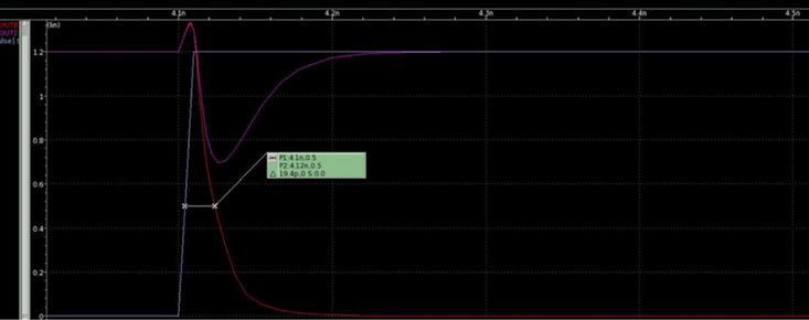
Figure 20: Sense amplifier delay on WaveView.
After determining our transistor sizes and sense amplifier delay, we can now proceed to the layout design. Similarly as the rest of the components, we just needed to make sure that the design passed DRC and LVS while still maintaining a small layout area (Figure 21).

Figure 21: Sense amplifier layout.
WRITE DRIVER:
The write driver (Figure 22) allows data to be read from an outside source and be written into a row of SRAM cells. The write drive only writes data when the Read/Write signal is logic level low. When the signal is logic level high the circuit doesn’t affect the bitlines. The reason for this is because of the tri-state buffers (Figure 23). When the Read/Write signal is logic level high this turns off the WE PMOS and WEB NMOS transistors which leaves the output as floating. The circuit consists of 4 inverters and 2 tristate buffers. This design allows us to write one bit, therefore we have 32 (Figure 24) instances so we can write 32 bits of data to any word line.

Figure 22: Write driver schematic.
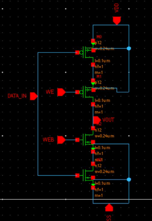
Figure 23: Tri-state buffer schematic.
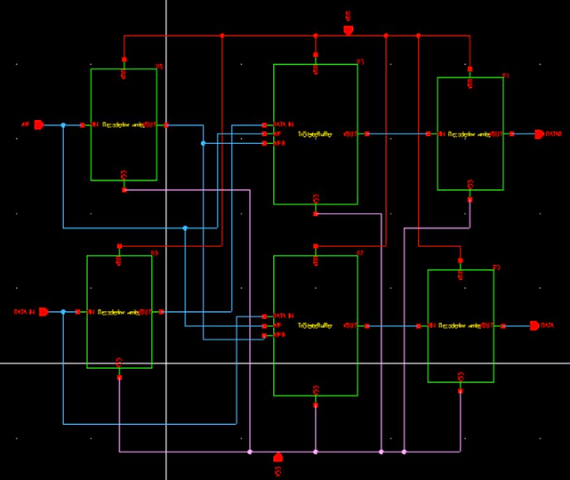
Figure 24: Schematic of one write driver cell.
After designing one cell, we tested the circuit in order to gather data about its operation. The read operation takes longer than the write operation, which means we had to ensure that our write driver was writing quickly. Figure 25, shows that it takes 216 ps to write which is faster than the 700 ps simulated read operation.

Figure 25: Write driver delay.
Next step after verifying our write driver is operating correctly is physical layout. Before we could design our Write Driver, we needed to design an inverter and a tristate buffer. Once those are completed, we create one cell (Figure 26). We use this one cell 32 times to make the complete Write Driver (Figure 27).

Figure 26: Write driver cell layout.

Figure 27: Portion of the write driver layout.
DECODER:
The decoder circuit (Figure 28) takes 6 address bits and decode that into 64 addresses. Each address will activate one row of 32 SRAM cells. Another feature of the decoder is that only one address can be selected at once. The design consists of 70 inverters, 12 NOR-2 logic gates, and 64 NAND-3 logic gates. We split the design into two stages. The first stage is a predecoder (Figure 29) and the second stage (Figure 30) decodes the signals from the predecoder. The reason we do this is to minimize the Fan-In of the second stage NAND gates in order to improve speed.
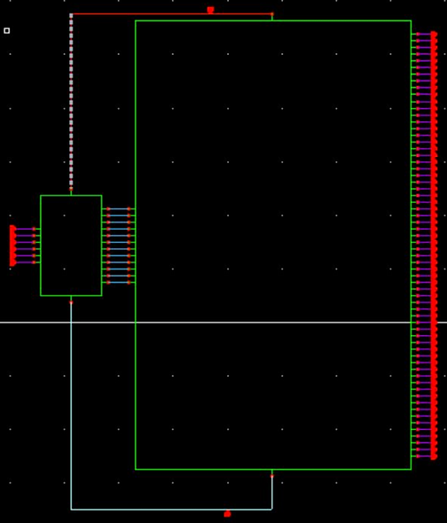
Figure 28: Address row decoder schematic.

Figure 29: One cell of predecoder circuit.

Figure 30: One cell of second stage of row decoder.
Since the Row Decoder is a large design we had to be careful with routing. We initially designed the Row Decoder all in on schematic which made for a messy design. Since our Row Decoder has two stages we design those two sub-circuits separately. This made the design easier to build and test. After design the two circuits we combined them in order to test the functionality of the circuit (Figure 31). Figure 31 shows the waveforms of the inputs and outputs of the circuit. Our testbench swept through every address which resulted in only one row being one at any given time. After that we obtained the delay of the circuit (Figure 32). Figure 32, shows the worst case delay of the Row Decoder. The reason we highlight the worst case delay is because this delay will make up the critical path which determines the maximum speed we can clock the SRAM.
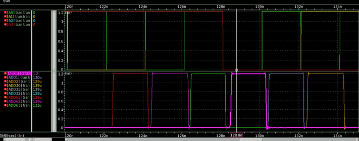
Figure 31: Verification of decoder functionality.

Figure 32: Worst case row decoder delay.
Our first design of resulted in a design that was huge. The decoder couldn’t line up with the SRAM array. The reason for this is because our NAND and NOR gates were extremely big. On our second attempt we used the fingering in order to keep the height the same as our SRAM cell. The difference was our design was wider. Figure 33 shows a portion of the final layout. One benefit of this design it made integrating the Row Decoder, the Mask and Buffer, and the SRAM array extremely easy.
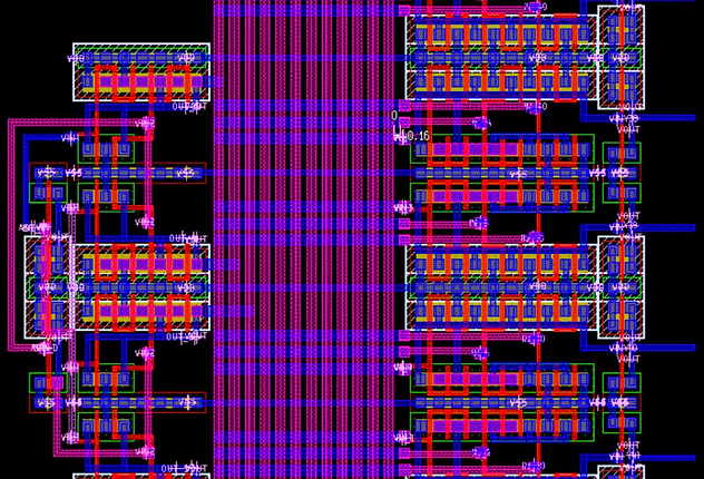
Figure 33: Portion of row decoder layout.
MASK AND BUFFER:
The job of the Mask and Buffer Circuit (Figure 34) is to keep the wordlines off while we are charging the bitlines during the read operation. The design of this circuit is 64 AND-2 logic gate (Figure 35) which consist of a NAND-2 logic gate and an inverter. Once again, we design our logic gates with the same height as the SRAM cell.

Figure 34: Portion of mask and buffer layout.

Figure 35: One cell layout of mask and buffer circuit.
CONTROLLER:
The control circuit enables both the pre-charge circuit and sense amplifier and tells the SRAM if it will perform a read or write operation. The controller block consists of two inputs, Clock and Read/Write (RW), and two outputs, Pre-Charged Enabled and Sense Enabled. The controller block consists of two symbols each designated for the pre-charge circuit (PC) and sense amplifier (SA) (Figure 36). These schematics consist of: a NAND gate, a NOR gate, buffers, and inverters. The buffers are used so that they can drive PC and SA.
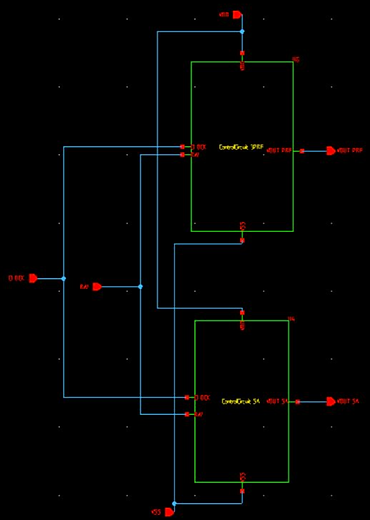
Figure 36: Controller box schematic.
As mentioned, our controller design contains two separate control boxes for the SA and PC. The sense enable control box has 15 inverters that cause the amount of delay for the SA to stay on (Figure 37). This can be tuned depending on how fast the SA needs to be enabled for. The box also has an inverter for the read and write input and a NOR gate. This causes the SA to be on only when the clock is at the falling edge and in read mode. The PC enable on the other hand has 5 inverters that cause the amount of delay the PC needs to charge the bitlines (Figure 38). It also consists of NAND gate and a read and write input. This means that the PC enable will only turn on if its on the positive edge and on read mode.

Figure 37: Sense amplifier enable schematic (ControlCircuit_SA).

Figure 38: Pre-charge enable schematic (ControlCircuit_3PRE).
For overall functionality of the controller, it needs to know if it is in the read or write operation. If it is in the write operation, the controller disables both the pre-charge circuit and the sense amplifier. If it is in read operation, the controller first enables the pre-charge circuit until the bitlines are charged to VDD. It then turns the pre-charge circuit off and enables the sense amplifier to output the voltage difference in the bitlines. This all occurs within one cycle. We created a testbench (Figure 39) to visualize these actions and the waveform can be seen in Figure 40. The last figure (Figure 41) shows the layout of the control circuit where the long stips of area are the inverters needed to meet the timing constraints.
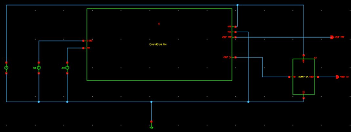
Figure 39: Controller testbench.

Figure 40: Controller enable measurements for pre-charge and sense amplifier.

Figure 41: Controller layout.
INTEGRATION:
After completing all individual components of the SRAM, it was now time to integrate them all together. This was an exciting milestone for us since we finally got the chance to see all of our hard work come together nicely to create the SRAM. We began with the schematic integration and recreated the top level architecture shown earlier in the report (Figure 1). Figure 42 shows the SRAM blocks wired together with labels to help recognize each component. We then began running some tests of the top level schematic for verification, but we weren't getting the expected values. All of our testbench and power results are explained in the following section of the report.
It was now time to begin integration of the layout and see if everything came together without any design issues. Fortunately, we did not run into any errors during the process. This was most likely because we did a good job on making sure our components were prepared to integrate with other components. One flaw that we did have was our write driver. As you can see in Figure 43, there is a huge chain of 32 write drivers taking up a large amount of area. We created the write driver without optimization because we were running out of time and needed to begin layout integration. Therefore we now call our layout design “The Boot” for laughs and giggles. Besides the large area, we managed to combine all the components and pass both DRC and LVS tests (Figures 44-46).

Figure 42: Top level schematic.
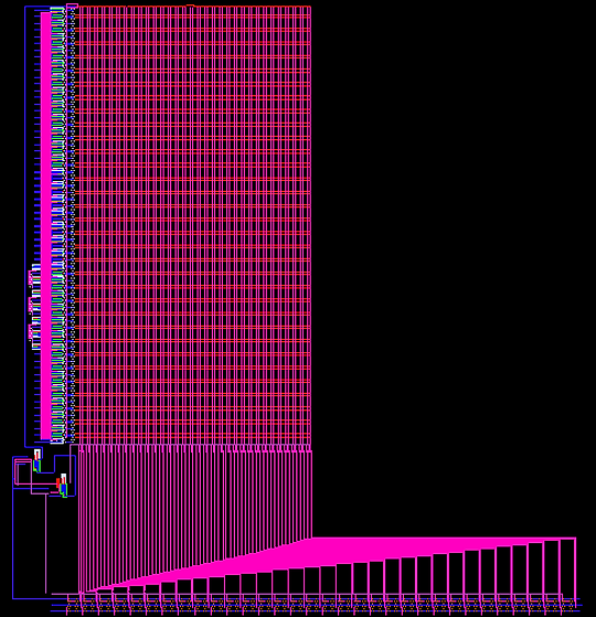
Figure 43: Top level layout ("The Boot").

Figure 44: Top level DRC report 1.

Figure 45: Top level DRC report 2.

Figure 46: Top level LVS report.
VERIFICATION AND RESULTS OF TOP LEVEL:
INPUT PATTERN TOP LEVEL FUNCTIONALITY

These are the inputs and outputs of our SRAM. We have the clock, data, addresses, read and write as our inputs. The outputs are the sense amplifier voltage outputs at address 0 and 63. The reason is that we are only writing and reading the data at these specific addresses.
The clock frequency we are using is 1 ns pulse width and the read and write have a 4 ns pulse width which activate the pre-charge and sense amplifier twice at read mode. The input data we have is 01011010 and it will be written to addresses 0 and 63.
AVERAGE ENERGY PER CYCLE
The average power is computed by dividing the active power to the clock frequency. We are averaging our power based on the clock frequency. We are supposed to be using 1 MHz for the competition but because the software crashes and wasn’t able to get a waveform so we are using 1 GHz instead.
Average power = 3.564 mW/1 Ghz = 3.564 nW/Hz
ACTIVE POWER
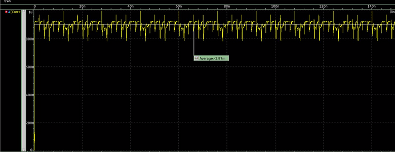
This is the current that is being drawn to the SRAM when it’s active. We will multiply the average current to VDD to get the active power of the SRAM. The clock we are using is at 1 Ghz.
Active power = 1.2 V * 2.97 mA = 3.564 mW
READ ACCESS TIME

The read access time is from 50% of the rising edge of the clock to the 50% of the rising edge of the output on the data bus. Our read access time is 1.21 ns. It also met the 100 mV bitline difference.
STANDBY POWER

To calculate the standby power we change all our inputs to zero except the power supply.
Power = 1.2 V * 435 uA = 522uW
DISCUSSION:
Our team took various engineering courses this semester and this was by far the most interesting one from them all, especially because of the course project. Although it was a bit challenging, we did gain a lot of knowledge from it and got a taste of what it feels like to be a designer in VLSI. We were introduced to the process of designing a memory chip using powerful Synopsys EDA tools. Some of the skills that we had to learn throughout the process include: learning how to navigate Custom Compiler, knowing how to create transistors using diffusion and poly layers, strategizing how to connect together the different components of the SRAM, and tuning transistor sizes for timing constraints.
Besides all the technical skills that we gained from the project, we also learned other types of skills. These include: team working, time management, and how to finish a full container of Advil in 2 days. This line of work is extremely tedious and took us countless hours of hard work to complete. Each SRAM component layout took at least 12+ hours to design and complete. But where we ran into trouble was the final integration of all the components. We managed to integrate all the pieces together in the schematic and the layout but when we ran the verification testbench, we were not getting the expected outputs. We began debugging procedures by monitoring each component at a time and seeing its performance. We then discovered a bug that made us discover even more bugs. First, we saw that the bitlines were not being charged completely to 1.2 V because the pre-charge circuit was not being enabled long enough. So we added some buffers to the control circuit so that it could keep the pre-charge circuit on for longer time but it only made a slight difference in the waveform.
We also noticed that the sense amplifier was turning on too late after enabling the wordline. The issue here is that once the wordline is turned on, that is when either bitline experiences the voltage difference. Which should be picked up by the sense amplifier after a
voltage difference of 100 mV. However, since the sense amplifier is being turned on too late, the voltage difference exceeds 100 mV which causes a write operation and flips the values stored inside the cell. So we sped up the clock so that the sense amplifier could turn on at the desired time, but unfortunately we were still encountering the same issue.
Although our top level design is outputting real values, these two bugs caused these values to be incorrect. We spent more than a week trying to fix these issues until we ran out of time. Which leads to our lesson of time management. It is always important to give yourself at least a 2-3 weeks window for debugging since nothing is ever expected to work on the first try. Besides this flaw, we still managed to get each component to function individually and pass both DRC and LVS tests which is still a huge accomplishment for us. If were given an additional 2 weeks of extra time to work on the project, we strongly believe that we could have gotten it completed.
Overall, this was a very exciting and enjoyable project to work on, especially since it is something that employers look for when applying for jobs. It was interesting to see the concepts learned in class being applied into the project. In most classes, we don't get that opportunity. Therefore, we would definitely recommend this course to anyone who is interested in the semiconductor industry or is seeking to learn the skills of being a chip designer at the transistor level.