Fixed Point MAC Unit

INTRODUCTION
The Fixed Point Multiply-Accumulate (FP MAC) unit is a fundamental block that multiplies two values and accumulates the results. Throughout the semester, we have been learning new material and working through homework problems to prepare us for the course project, therefore, the purpose of this project will be to implement the FP MAC unit onto a FPGA board. This will also include implementing a Finite State Machine (FSM) to control the unit, which will be displayed onto a LCD screen through an Arduino, and a SRAM model to store input values from a 4x4 Numerical Keypad. All code in the FPGA board will be written in Verilog on Quartus Prime Lite and all code in the Arduino will be written in C language. The FP MAC unit is used for Digital Signal Processing (DSP) applications such as in Artificial Intelligence (AI) Engines.
DESIGN IMPLEMENTATION
MATERIAL:
-
Terasic DE10-Lite FPGA
-
Arduino UNO
-
20x4 LCD
-
4x4 Numerical Keypad
-
Jumper Cables
TOP LEVEL MODULE IMPLEMENTATION:
The top level module will contain all the design sub-modules used in the project. It defines inputs and outputs, includes instances of sub-modules, handles the wiring from sub-module to sub-module, and initializes signals. Furthermore, the top level module will sometimes include sequential and combinational logic that connect to or control the submodules. In our design, we include the FSM model and Read/Write SRAM model in the top level hierarchy.
SRAM SUB-LEVEL MODULE IMPLEMENTATION:
The memory block will be a 8x16-bit Static Random Access Memory (SRAM) with a 3-bit Address input signal, three 1-bit active low control signals, and a 16-bit bi-directional data signal (Figure 1). The address signal needs to be 3-bits because there are 8 16-bit memory locations (23 = 8) to choose from. The three input control signals are Chip Select (nChip_S), Write Enable (nWE), and Output Enable (nOE). Whenever we are using the SRAM block, we will need to enable the nChip_S and either nOE or nWE to read or write. The 16-bit IO (Input/Output) signal will input and output data depending on whether we are in read or write mode. The project will be using two SRAMS, SRAM A and SRAM B, to store multiple input values from the 4x4 numerical keypad.
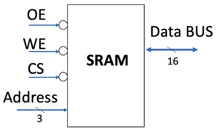
Figure 1: 8x16-bit SRAM Block.
This Verilog code will include a section for read operation and for write operation (Figure 2). To read from the RAM, nChip_S and nOE will need to be low (enabled) and nWE will need to be high (disabled). If this is true, the RAM data will be assigned to IO, if not, IO will be at a high-impedance state. To write to the SRAM, a similar approach will be used but instead nWE will need to be enabled and nOE disabled. This will be written in an always block because we are going to writing data from the IO wire to the RAM data, which is a register.
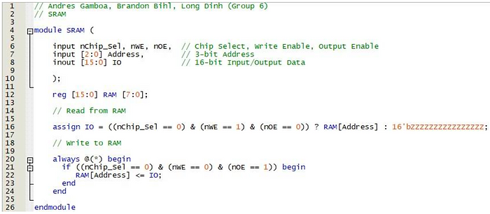
Figure 2: SRAM Sub-Module Verilog Code.
FSM AND READ/WRITE SRAM MODEL IMPLEMENTATION:
The Finite State Machine will have 4 states and will be controlling whether to read or write from the SRAM (Figure 3). The first state (S0) will be the “Reset” state which resets all the SRAM values to zero. The second state (S1) will be the “SRAM A Input” state which saves input values from the keypad into SRAM A and displays the value onto the 7-segment display. The third state (S2) will be the “SRAM B Input” state which saves input values from the keypad into SRAM B and displays the value onto the 7-segment display. The final state (S3) will be the “FP MAC Calc” state which fetches data from SRAM A and SRAM B and inputs it into the MAC unit and displays the result onto the 7-segment display. To move from one state to another, we will need to press one of the buttons on the FPGA.

Figure 3: 4-State Finite State Machine.
The SRAM model includes a Data register, Control unit, Memory Address register, and SRAM block (Figure 4). The Control unit will be the FSM, and will control all signals in the model. The signals from the FSM to the Data register will include, Write & Read_Data, Disp_Data, Mul_Data, Disp_MAC, and Reset_Data.

Figure 4: Read/Write SRAM Model.
The Data register is essentially the gatekeeper to send or receive data to or from the SRAM. For example, when Write_Data_A is enabled, values that are entered from the keypad will be equal to the Data_A bus, which will also be connected to IO to store them into SRAM_A. When Read_Data_A is enabled, Data_A bus will read the data from SRAM_A. When Disp_Data is enabled, it will display the data that is currently in the Data_A bus. When Mul_Data_A is enabled, the data that is in the Data_A bus will be inputted into the MAC unit, and the result will be displayed on the 7-segment display when Disp_MAC is enabled. Lastly, when Reset_Data_A is enabled, the value stored in the Data_A bus will be set to zero. Figure 5 shows the verilog code written for the Data Register.

Figure 5: Data Register Verilog Code.
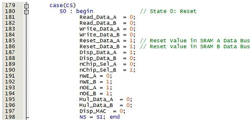
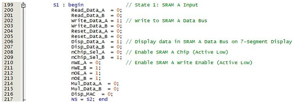
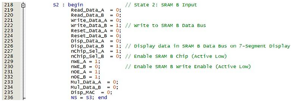
Figure 6 shows the Verilog codes of each state and the signals that are enabled at each state. S0 will enable the Reset_Data signals to reset the values stored in the SRAMs. S1 will enable the Write_Data_A, Disp_Data_A, nChip_Sel_A, and nWE_A signals to store the values from the keypad into SRAM A and display it onto the 7-segment display. S2 will be similar as in S1 except that it will now be for SRAM B. S3 will enable Mul_Data signals to fetch the data from Data_A and Data_B to input into the MAC unit. The Disp_MAC signal is also enabled to display the result of the MAC calculations onto the 7-segment display.
a)
Figure 5: Cache Simulator Diagram.
b)
c)

d)
Figure 6: Verilog code for State a) 0 b) 1 c) 2 d) 3.
KEYPAD TO FPGA IMPLEMENTATION:
The keypad consists of 16 buttons and 8 wires, therefore a method of multiplexing is required to distinguish which signal is intended (Figure 7). We set the four rows as inputs, the four columns as outputs, and use the FPGA’s built in 50 MHZ clock as an input. We also used inter-nested case statements to cycle through each possible scenario every millisecond to determine the user's intended command. This is achieved by driving the row high and the column low. When the user presses a button, the inter-nested case statement will select the intended row while the outer case statement will be selected if the column for that corresponding row is selected. Using a lag time delay will ensure the intended button was selected to avoid any undesired glitches. Figure 8 shows a portion of the Verilog code for the keypad implementation.
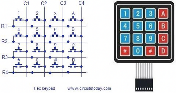
Figure 7: Matrix for the 4x4 Numerical Keypad.
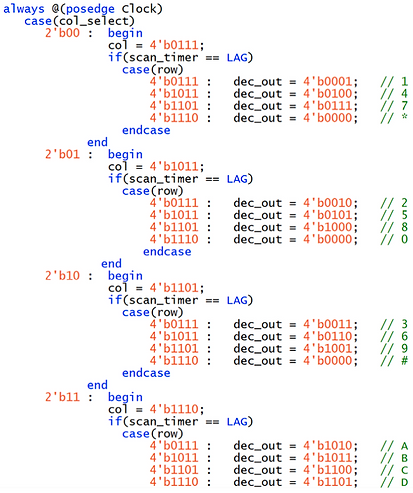
Figure 8: Portion of the Keypad Verilog Code.
FIXED POINT MAC IMPLEMENTATION:
-
16-Bit Adder
-
In our design, the 16-bit adder (Figure 9) has two input ports (a and b) and one output port (sum). Internally, this adder consists of Full Adders that are cascaded to 16 bit. Thus, the logic of this addition is very similar to the traditional logic adder. However, this adder has a function to set the result to saturation when the overflow is detected.
-
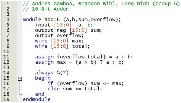
Figure 9: 16-bit Adder Verilog Code.
16-Bit Multiplier
-
-
Normally, a multiplication of two 16-bits inputs will produce the output of 32 bits. We were able to produce the output as 16-bit by truncate method. In which, we pick 7 bits from the left of the binary point and 9 bits from the right of the binary point as the final result. The remaining fractional bits are removed after performing rounding. Figure 10 shows the Verilog code for the 16-bit multiplier.
-

Figure 10: 16-bit Multiplier Verilog Code.
7-SEGMENT DISPLAY IMPLEMENTATION:
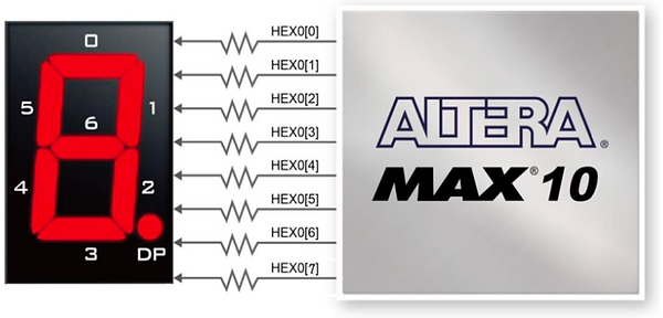
The 7-Segment implementation takes a 16-bit input signal and gets broken up into four 4-bit sections since each 7-segment only displays 4-bits in hexadecimal. For example the hex3 will display bits 15-12, hex2 will display bits 11-8, hex1 will display bits 7-4, and hex0 will display bits 3-0. These 4-bit values are each inputted into a case statement which determines which number to display on the segment (Figure 11) . The 7-segment displays are active low.
a)

b)
Figure 11: a) 7-Segment Display and b) Portion of 7-Segment Verilog Code.
FPGA TO ARDUINO INTERFACE:
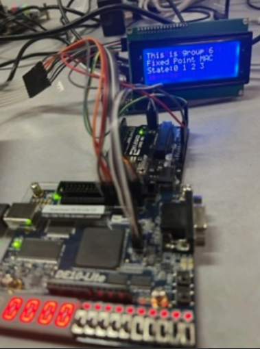
We intended on interfacing the FPGA and the Arduino using the Serial Peripheral Interface (SPI). This could be achieved using 4 wires including a clock signal sent from the master to the the slave, MOSI (master out- slave in), MISO (master in- slave out) and a SS (Select Signal). In theory, the master should initiate the communication by activating the SS, which would start the slave to drive its MISO output while the master drives its MOSI output. On the falling edge of the clock, both master and slave will drive their most significant bit (MSB). On the rising edge, the master and slave input the corresponding signal into the least significant bit (LSB). The process would continue until all bits are transmitted, then the SS would be deactivated by the master. The Arduino is responsible for controlling the 20x4 LCD, which displays our group name, the name of our project, and the 4 States (Figure 12).

a)
b)
Figure 12: a) Arduino schematic and b) LCD Interface with FPGA.
SIMULATION RESULTS AND DISCUSSION
Figures 13 and 14 are the simulation results for adder and multiplier. The results are correct and show the expected output. For instance, input of a = 16’h1B00, and b =16’h FE80, the sum = 16’hFE80. This value is matching with the homework solution. In addition, case a = 16’h1000, and b =16’hFFFF, the result output is saturated and shown as sum = 16’hFFFF. Another example of multiplication, we input hex value of a = 1B00 and b = FE80, the output value shows the correct value 6BC0, which is the 16-bit that is after rounding.

Figure 13: 16-Bit Adder Output Simulation.

Figure 14: 16-Bit Multiplier Output Simulation.
We were able to get working results but not necessarily how we intended. Beginning with not being able to successfully interface the Arduino with the FPGA board. We tried using SPI protocol, but we were not able to get it to work even after attempting multiple approaches. Therefore to replace the LCD, we used the last 7-segment display (hex5) to display the current state.
We were able to get the MAC unit to work correctly and were able to confirm by running a simulation on Icarus Verilog software. However, when we integrated it with the overall design, we were not getting the expected results, but there was multiplying and accumulating taking place. We were also unable to integrate the pipeline into our design but it can be done by adding registers to break the critical path into segments to help optimize our design and to decrease computation time. We also used a button for asynchronous reading and writing which seemed to work correctly.
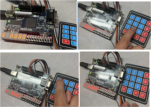
Figure 15: Demonstration of the 4 States.
CONCLUSION:
This project was a great opportunity in interfacing multiple components and to demonstrate the ability to code in Verilog. This was also a great opportunity in learning how to delegate work upon team members and also how to integrate our individual work to a team assignment. An issue that we had was connecting interfacing the Arduino and FPGA using the SPI connection. A potential resolution to this issue can be to use the UART protocol. Despite not getting the FPGA to interface with the Arduino we were able to successfully simulate our working code using Icarus Verilog software. Overall, we enjoyed working on this project, even though we did not get the expected results, but we were able to learn a lot throughout the process and see how the concepts learned in class are implemented into real world applications.