Dot Product Benchmark of MIPS
ISA with Forward Chaining &
2-Bit Branch Predictor

INTRODUCTION
One family of the Reduced Instruction Set Computer (RISC) instruction set architectures (ISA) is the Million Instructions Per Second (MIPS) Processor. In Project 1, we implemented a sub- set of the MIPS ISA that can execute a dot product benchmark program using Verilog. The design consisted of taking two vectors stored in memory, performing dot product, and storing the summation in the Register File. In Project 2, we will now need to make the MIPS architecture pipelined and add the forward chaining and 2-bit branch predictor techniques into the design. These techniques were introduced in class, and it is important that we now attempt to implement it to ensure a full understanding.
DESIGN/ARCHITECTURE/ALGORITHM DESCRIPTION
PIPELINED MIPS STAGES:
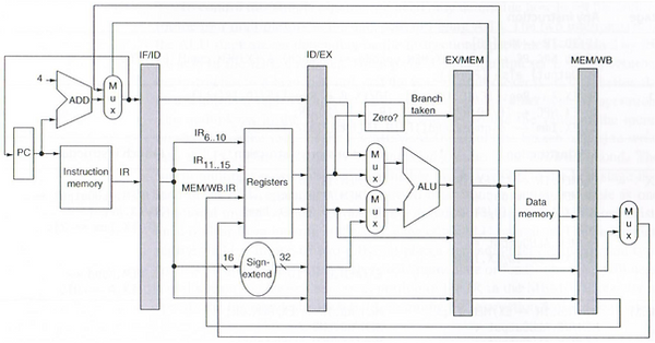
The MIPS architecture consists of 5 stages which include Instruction Fetch (IF), Instruction Decode (ID), Execute (EX), Memory (MEM), and Write-Back (WB). In the IF stage, the program counter (PC) is used to determine which instruction to fetch from the instruction memory. The instructions contain all the information needed by the remaining stages such as opcodes, registers, and immediate values. The 2-bit Branch Predictor will be included in this stage. The ID stage uses the instruction data to select the desired registers from the Register File (RF), sign extend 16-bit immediate values to 32-bits, and determine the desired control signals for the 5 stages. In the EX stage, the Algorithmic Logic Unit (ALU) performs operations between registers or registers and immediate values. These operations are determined by the opcode encoded in the instruction data. The zero_flag indicator, used for branching operations, will be set to high when comparing a register value to zero. This stage will also contain the Forward Chaining Unit, which will be discussed later in the report. The MEM stage allows for data memory access when using load or store instructions. The last stage is the WB stage, which sends either the contents within the data memory or results from the ALU back into the FR. Figure 1 shows an overview of the MIPS architecture and each of the 5 individual stages.

Figure 1: MIPS Architecture.
FORWARD CHAINING AND 2-BIT BRANCH PREDICTOR:
Forward Chaining is a method used to prevent Data Hazards which occur when there is data dependency between instructions. The 3 types of data hazards that we have learned in class are Read After Write (RAW), Write After Read (WAR), and Write After Write (WAW). RAW occurs when Instruction 2 tries to read a register before Instruction 1 writes to it. WAR occurs when Instruction 2 tries to write to a register before Instruction 1 reads from it. WAW occurs when Instruction 2 tries to write to a register before Instruction 1 writes to it.
With Forward Chaining, we forward the Instruction 1 data directly to the Execution Stage of Instruction 2. This allows for Instruction 2 to proceed with the ALU operation without needing wait for Instruction 1 to finish and stall for a number of clock cycles. Figure 2a shows how Data Hazards occur and Figure 2b shows how Forward Chaining can fix them.

a)

b)
Figure 2: a) Data Hazards and b) Forwarding to avoid Data Hazards.
2-Bit Branch Predictor is a method used to reduce the number of Branch stalls. This can be done by estimating whether the branch is Taken or Not Taken and computing the Taken Branch address sooner. The 2-Bit prediction scheme consists of 4 states: Strongly Taken, Weakly Taken, Strongly Not Taken, and Weakly Not Taken (Figure 3). If you initially predict that the branch is Taken, you begin at the Strongly Taken state (11). If the prediction is correct, you stay at that state, else you move onto the Weakly Taken state (10). If the prediction is correct, you move back to the Strongly Taken state, else you move onto the Strongly Not Taken state (00). In this state, you are now predicting that the branch will not be taken. Similarly, if you are correct, you stay at that state, else you move onto the Weakly Not Taken state (01). If you are wrong again, you will need to change you prediction again to Taken.

Figure 3: Basic 2-Bit Branch Predictor.
TASK:
The goal for Project 2 is to implement a sub-set of the MIPS ISA using Verilog that executes a dot product benchmark program (Figure 4). The design will need to be pipelined and contain Forward Chaining and 2-Bit Branch Predictor techniques. The program consists of 11 instructions that takes two vectors stored in memory, performs dot product, sums the results, increments the vectors by 4, and loops for a number of iterations. Vector A will be our student ID number and Vector B will be our student ID number but with each digit incremented by the last digit of our student ID. In my case, vector A will be XXXXXXXXX and vector B will be XXXXXXXXX. Note that I have censored my student ID for privacy reasons.

Figure 4: Dot Product Benchmark Program.
DESIGN PROCESS:
In order to make the coding process simpler and easier to follow, I began by first creating an RTL diagram to visualize what contents will be going into each stage and all the signals that will be needed. The diagram is shown in Figure 5 with IF signals shown in Orange, ID signals shown in Green, EX signals shown in Red, MEM signals shown in Purple, WB signals shown in Dark Blue, and Control Signals shown in Light Blue. The Black registers in between each state are the Pipeline Register also known as Buffer Registers.

Figure 5: RTL Diagram of MIPS Architecture.
In the IF stage, I have 4 input signals (Jump, jp_addr, br_cond, br_addr) that determine whether the Program Counter (PC) will be a Jump Address, Branch Address, or the Next Program Counter (NPC = PC + 4). The 8 LSB of the PC are used to determine which instruction to read from memory. At the positive clock edge, the selected instruction and NPC (ip_npc) are stored into the IF/ID Buffer. These register values will be used as inputs in the following stage.
In the ID stage, the instruction signal will be broken up into different signals since it contains information needed for the following stages. Using the 32-bit instruction signal, I can connect a wire for the opcode (bits 31-26), function (bits 5-0), source register (bits 25-21), target register (bits 20-16), destination register (bits 15-11), immediate value (bits 25-0), and jump address (bits 25-0). The control unit is implemented in this stage and outputs all the control signals to the other stages in respect to the opcode and function encoded in the instruction data. When the Read Register signal is high (RegRead), the register will read the value stored in the register and store it into the ID/EX Buffer. When the Write Register signal is set high (RegWrite), it will take the input data coming from the Write Back stage (wb_data) and store it into the Register File (RF) Address (rf_addr). There are also certain signals that are simply passed from the IF/ID Buffer to the ID/MEM Buffer.
In the EX stage, I implement the branching and jumping addresses (ex_br_addr and ex_jp_addr), determine the RF Address (ex_rf_addr), perform ALU operations, and implement the Forward Chaining Unit. The Forwarding Unit takes the input Source and Target registers (ex_reg_s and ex_reg_t) and compares them with the RF Write Addresses from the MEM and WB stages (mem_rf_addr and wb_rf_addr). If any of the registers match, the Forwarding Unit will forward the data from either the MEM stage (mem_alu_results) or WB stage (wb_data_Frwd) into the input of the ALU. If none of the registers match, the ALU will input the data read from the RF (data_a or data_b) or an immediate value (src_imm). All output signals are stored in the EX/MEM Buffer.
The MEM stage is where majority of the signals are fed back into a previous stage such as jump control signal (Jump), MEM Forward enable signal (MemForward), Branch Address (br_addr,), ALU results (mem_alu_results), RF Write Address (mem_rf_addr), and Jump Address (jp_addr). In this stage the Branch control signal (Branch) and the zero_flag are AND’ed together which output the Branch Condition signal (br_cond) that is fed back to the IF stage. When the Memory Read signal is high (MemRead), the data from the data memory will be read and stored into the MEM/WB Buffer. When the Memory Write signal is high (MemWrite), it will take the input data (ex_data_b) and store it into the Data Memory Address (dm_addr) which is the 8 LSB of the ALU results.
In the WB stage, I have a control signal (MemtoReg) that determines which data to write back to the ID stage and/or EX stage when forwarding is enabled. This data is either the data from the Data Memory (dm_data) or the results from the ALU (dm_alu_results). The WB Forward enable signal (WBForward) is fed back to the Forward Unit in the EX stage along with the write back data (wb_data_Fwrd). The Register Write enable signal (RegWrite) and write back data (wb_data) are fed back to the ID stage.
SIMULATION/VERIFICATION
Unfortunately, I was not able to implement the 2-Bit Branch Predictor as I ran out of time. The Predictor would have been implemented in the IF stage using the 4-state scheme. However, I was able to convert the non-pipelined Mini-Project 1 design to pipelined and implement the Forward Chaining technique. It was a rigorous task to perform because I now had multiple things happening simultaneously and multiple wires connecting between different stages. I slightly struggled when implementing the Forward Chaining Unit because the desired data was not being forwarded to the inputs of the ALU especially after the Load instruction. Therefore, I had to modify the Forward Chaining Unit by adding if statements and adding a wire directly from the output of the Data Memory to the input of the ALU. Although I did find myself struggling in other areas of the design, I found keeping track of all the signals to be the hardest task, especially when making the top-level connections in the Top Module. Luckily, the RTL diagram that I made helped me keep track of all the signals.
Figure 6 shows the simulation results of the of the design. Figure 6a shows the non-pipelined waveforms from Mini-Project 1 where the final result of the dot product (157) was computed around 4100 ns. Figure 6b shows the pipelined waveforms with Forward Chaining where the final result (179) was computed around 1080 ns, which is almost 4 times faster than the non- pipelined version. We can confirm that the result is correct by performing the dot product manually:
Vector A: XXXXXXXXX (my Student ID)
Vector B: YYYYYYYYY (each number of my Student ID + 8)
Result = (XxY) + (XxY) + (XxY) + (XxY) + (XxY) + (XxY) + (XxY) + (XxY) + (XxY)
Result = (Z) + (Z) + (Z) + (Z) + (Z) + (Z) + (Z) + (Z) + (Z)
Result = 179
Note that X, Y, and Z are not unique are are used to censor my Student ID.
Figure 7 shows the simulation log which displays the input register values of each stage at each clock signal. I have included the section that displays the dot product final result from the ALU (179) which gets written to Register 1 during the WB stage (circled in Red).

a)

b)
Figure 6: Simulation Waveforms of a) non-pipelined design and b) pipelined design with Forward Chaining.

Figure 7: Simulation Log Showing Stored Register Values in Each Stage.
CONCLUSION:
Project 2 is a great opportunity for students to further their understanding of the MIPS Architecture even more by converting the design from non-pipelined to pipelined and adding additional techniques to improve the throughput of the design. Although learning the concepts in class are useful, being able to implement them in Verilog ensures a full understanding. I found this project to be slightly challenging because I had to keep track of all the signals and ensure that they were connected in the correct location and triggered at the appropriate time. This cautious task consumed a lot of my time which ultimately led to me not being able to implement the 2-Bit Branch Predictor. If I had more time on the project, I would have completed the Branch Predictor and tested other benchmark programs. However, even with only the pipelined design and Forward Chaining, I was able to reduce the number of clocks substantially, showing how efficient your design can become with these techniques. Overall, I enjoyed working on this project and believe it is an essential assignment because it helped me further my understanding of the MIPS architecture and improve my Verilog coding skills.